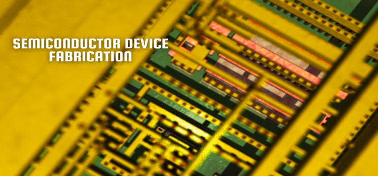
Semiconductor device fabrication is the intricate process of creating semiconductor devices, specifically integrated circuits (ICs), that are commonly found in everyday electronics like computer processors, microcontrollers and memory chips (including NAND flash and DRAM). This process involves multiple steps of photolithography and physio-chemical processes like thermal oxidation, thin-film deposition, ion-implantation, and etching. These steps gradually form electronic circuits on a wafer made of pure single-crystal semiconducting material, with silicon being the most commonly used material, although compound semiconductors may be used for specific specialized applications.
The process of manufacturing semiconductors takes place in specialized facilities commonly referred to as “fabs” or foundries, which house the essential “clean rooms”. For highly advanced semiconductor devices like those in 14/10/7 nm nodes, the fabrication process can last up to 15 weeks, with 11-13 weeks being the average duration in the industry.
Nowadays, the semiconductor industry is a globalized business. Key semiconductor manufacturers usually have production facilities in different regions worldwide. Samsung Electronics, the primary semiconductor manufacturer globally, operates facilities located in South Korea and the US. Intel, the second-largest manufacturer, has facilities across the US, Europe, and Asia. Meanwhile, TSMC, the world's most significant pure-play foundry, has facilities in Taiwan (China), Mainland China, Singapore, and the US. On the other hand, Qualcomm and Broadcom, major fabless semiconductor companies, sub-contract their production to firms such as TSMC, while operating facilities distributed across various countries.

The leading countries in semiconductor device fabrication include the United States, Japan, Taiwan (China), South Korea, and Mainland China. These countries have established advanced semiconductor industries with state-of-the-art manufacturing facilities and a talented workforce. The United States is home to many large semiconductor companies, such as Intel and Texas Instruments, while Japan is known for its high-quality and high-performance memory products. Taiwan (China) and South Korea are important semiconductor manufacturing hubs, with companies such as TSMC and Samsung dominating the foundry market. Mainland China is also rapidly expanding its semiconductor industry, with a growing number of domestic companies like SMIC and the government investing heavily in research and development.
In 2019, various chip manufacturers such as Intel, UMC, TSMC, Samsung, Micron, SK Hynix, Toshiba Memory and GlobalFoundries were mass producing 14 nanometer and 10 nanometer chips. TSMC and Samsung were also in mass production of 7 nanometer process chips, however, their definition of the 7 nanometer node was similar to Intel's 10 nanometer process. Samsung began production on their 5 nanometer process in 2018. As of 2019, TSMC's 5 nanometer N5 node had the highest transistor density, with 171.3 million transistors per square millimeter. Both Samsung and TSMC planned to produce 3 nanometer nodes in 2019. In order to save resources, GlobalFoundries made the decision to halt development of new nodes beyond 12 nanometers, as setting up a new fab to handle sub-12 nm orders would be outside the company's financial capabilities.
Producing 3 nm technology is currently being developed by semiconductor manufacturers such as TSMC (Taiwan) , Samsung (South Korea) , Intel, and GlobalFoundries (United States). These companies are investing heavily in their research and development efforts to make this technology a reality. However, it is a complex process and still in the early stages, so it may take some time before it becomes widely available.
Semiconductor device fabrication involves four main categories of processing steps: deposition, removal, patterning, and modification of electrical properties. Deposition includes processes such as physical vapor deposition, chemical vapor deposition, and atomic layer deposition that transfer materials onto the wafer. Removal involves processes like wet or dry etching and chemical-mechanical planarization that remove material from the wafer. Patterning involves shaping or altering deposited materials, typically through lithography techniques. Modification of electrical properties includes doping and annealing processes, and can also involve reducing a material's dielectric constant through UV processing. These steps are often carried out through oxidation to create semiconductor-insulator junctions, such as in the local oxidation of silicon for metal oxide field effect transistors. In modern chips, there can be up to 11 or more metal levels produced through over 300 sequenced processing steps.